Connections
Information from the butterfly and mega169 datasheets…
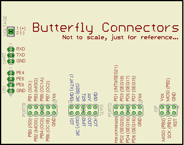
Lookie! my first Eagle drawring:
PortB pin connections
Connected to the Port B header, ISP header, Dataflash, and Joystick. Note that for joystick buttons, “The common line of all directions is GND. This means that internal pull-up must be enabled on the ATmega169 to detect the input from the joystick.”
| ’'’Pin’’’ | ’'’Alias’’’ | ’'’Connected to…’’’ | ||||
| PB0 | !SS/PCINT8 (SPI Slave Select input or Pin Change Interrupt8) | Dataflash CS pin | ||||
| PB1 | SCK/PCINT9 (SPI Bus Serial Clock or Pin Change Interrupt9) | Dataflash SCK pin, ISP Header (pin 3) | ||||
| PB2 | MOSI/PCINT10 (SPI Bus Master Output/Slave Input or Pin Change Interrupt10) | Dataflash SI pin, ISP Header (pin 4) | ||||
| PB3 | MISO/PCINT11 (SPI Bus Master Input/Slave Output or Pin Change Interrupt11) | Dataflsah SO pin, ISP Header (pin 1) | ||||
| PB4 | OC0A/PCINT12 (Output Compare and PWM Output A for Timer/Counter0 or Pin Change Interrupt12) | Joystick center (O) | ||||
| PB5 | OC1A/PCINT13 (Output Compare and PWM Output A for Timer/Counter1 or Pin Change Interrupt13) | dunno!! | ||||
| PB6 | OC1B/PCINT14 (Output Compare and PWM Output B for Timer/Counter1 or Pin Change Interrupt14) | Joystick up (A) | ||||
| PB7 | OC2A/PCINT15 (Output Compare and PWM Output A for Timer/Counter2 or Pin Change Interrupt15) | Joystick down (B) |
PortD pin connections
Connected to the Port D header and the LCD panel.
| ’'’Pin’’’ | ’'’Alias’’’ | ’'’Connected to…’’’ | ||||
| PD0 | ICP1/SEG22 (Timer/Counter1 Input Capture pin or LCD front plane 22) | LCD15 | ||||
| PD1 | INT0/SEG21 (External Interrupt0 Input or LCD front plane 21) | LCD16 | ||||
| PD2 | SEG20 (LCD front plane 20) | LCD18 | ||||
| PD3 | SEG19 (LCD front plane 19) | LCD13 | ||||
| PD4 | SEG18 (LCD front plane 18) | LCD11 | ||||
| PD5 | SEG17 (LCD front plane 17) | LCD12 | ||||
| PD6 | SEG16 (LCD front plane 16) | LCD14 | ||||
| PD7 | SEG15 (LCD front plane 15) | LCD9 |
PortE pin connections
Connected to USI header, the Joystick, the Dataflash, and UART circuitry.
Note that pins 4-6 are connected to the USI header and nothing else. If you aren’t using USI, these pins might be convenient to use for other purposes.
| ’'’Pin’’’ | ’'’Alias’’’ | ’'’Connected to…’’’ | ||||
| PE0 | RXD/PCINT0 (USART Receive Pin or Pin Change Interrupt0) | UART circuit | ||||
| PE1 | TXD/PCINT1 (USART Transmit Pin or Pin Change Interrupt1) | UART circuit | ||||
| PE2 | XCK/AIN0/ PCINT2 (USART External Clock or Analog Comparator Positive Input or Pin Change Interrupt2) | Joystick left (C) | ||||
| PE3 | AIN1/PCINT3 (Analog Comparator Negative Input or Pin Change Interrupt3) | Joystick right (D) | ||||
| PE4 | USCK/SCL/PCINT4 (USART External Clock Input/Output or TWI Serial Clock or Pin Change Interrupt4) | USI Header (pin 1) | ||||
| PE5 | DI/SDA/PCINT5 (USI Data Input or TWI Serial DAta or Pin Change Interrupt5) | USI Header (pin 2) | ||||
| PE6 | DO/PCINT6 (USI Data Output or Pin Change Interrupt6) | USI Header (pin 3) | ||||
| PE7 | PCINT7 (Pin Change Interrupt7), CLKO (Divided System Clock) | Dataflash reset pin |
PortF pin connections
Connected to the temperature circuit, voltage reader circuit, light sensor circuit, and JTAG header.
Note that if you aren’t using the JTAG interface, pins 4-7 might be convenient to use for other purposes.
| ’'’Pin’’’ | ’'’Alias’’’ | ’'’Connected to…’’’ | ||||
| PF0 | ADC0 (ADC input channel 0) | Temperature sensor circuit | ||||
| PF1 | ADC1 (ADC input channel 1) | Volatage reader circuit | ||||
| PF2 | ADC2 (ADC input channel 2) | Light sensor circuit | ||||
| PF3 | ADC3 (ADC input channel 3) | VCP - VC-peripheral output, connected to the light sensor and temp sensor | ||||
| PF4 | ADC4/TCK (ADC input channel 4 or JTAG Test ClocK) | JTAG header (pin 1) | ||||
| PF5 | ADC5/TMS (ADC input channel 5 or JTAG Test mode Select) | JTAG header (pin 5) | ||||
| PF6 | ADC6/TDO (ADC input channel 6 or JTAG Test Data Output) | JTAG header (pin 3) | ||||
| PF7 | ADC7/TDI (ADC input channel 7 or JTAG Test Data Input) | JTAG header (pin 9) |